We sat down with Jim Chiu, the Founder and CEO of Holonomy Systems, to discuss the company’s current work and its long-term vision for accelerating fusion development.
Holonomy Systems is building the Photon Brick, a standardized laser pump module designed around surface-emitting architectures for inertial confinement fusion and defense applications. The company integrates power electronics and per-shot telemetry into each unit to enable predictive maintenance and higher reliability than traditional edge-emitting diode systems. This platform leverages advanced semiconductor packaging in Taiwan and intellectual property management in the United States to scale high-power laser production for the global energy market.
Holonomy Systems is building the Photon Brick. Can you explain what the Photon Brick is and how it fits into diode laser architectures?
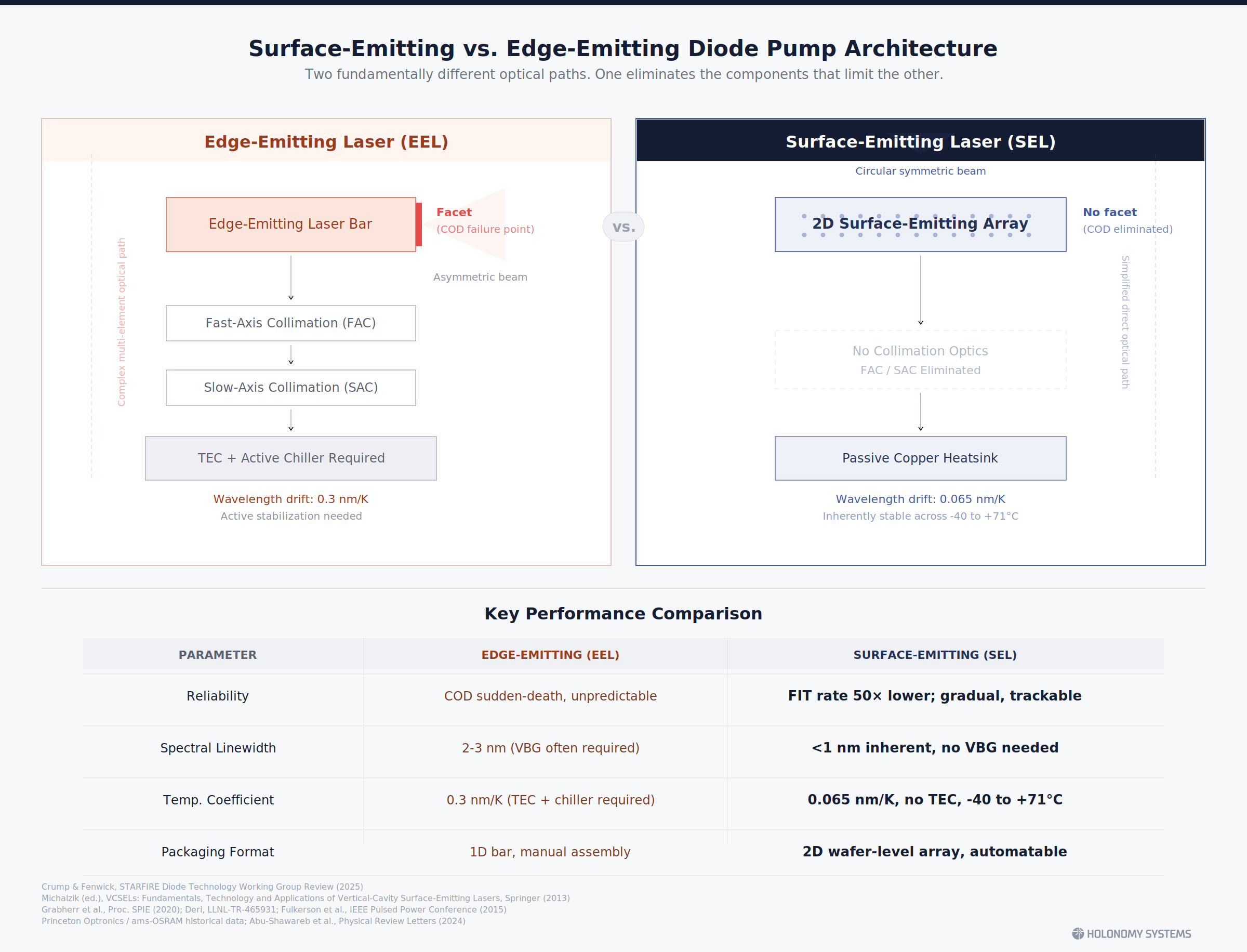
A laser system follows the same physical chain whether it is a rangefinder on a ground vehicle or a driver for a fusion power plant: electrical power goes in, photons come out. Somewhere in that chain sits a pump source, a semiconductor diode that converts electricity into the light that energizes the laser's gain medium. Today, pump modules are available as catalog products, but they are passive optical sub-assemblies built around edge-emitting laser bars. They inherit the constraints of that architecture: asymmetric beams requiring multi-element collimation optics, facets susceptible to catastrophic optical damage, temperature sensitivity requiring active cooling, and one-dimensional bar formats that limit packaging density.
The Photon Brick starts from a different premise. Our thesis is that surface-emitting laser architectures, VCSELs and the emerging class of photonic crystal surface-emitting lasers, offer structural advantages for pump module design that the edge-emitting paradigm cannot replicate. Surface emitters produce circular symmetric beams, eliminate the facet failure mechanism entirely, and operate across wide temperature ranges without active wavelength stabilization. These are not incremental improvements to the existing approach. They are physical properties that flow directly from the geometry of surface emission, and they have direct consequences for how a pump module can be packaged, tested, and maintained at scale.
On top of that physical foundation, the Photon Brick integrates everything between raw DC power and calibrated photon output into a single module: pulse drive electronics, thermal management, beam conditioning, and a per-shot intelligence layer that captures the electrical and optical signature of every pulse. The customer interface is simple. DC power and a digital command go in. Calibrated, characterized pump light comes out. The system integrator never has to manage diode drive waveforms, thermal stack-ups, or optical alignment.
If that thesis holds, four properties follow. First, the absence of facets eliminates catastrophic optical damage, the dominant sudden-death failure mode in edge-emitting pump diodes, reducing failure rates by roughly 50 times. Second, surface-emitting cavities produce an inherently narrow spectrum of less than 1 nm, compared to 2 to 3 nm for edge emitters, which means tighter wavelength matching to the gain medium's absorption band. Third, the low wavelength temperature coefficient of 0.065 nm per degree, versus 0.3 nm per degree for edge emitters, enables operation from minus 40 to plus 71 degrees Celsius without thermoelectric coolers, eliminating a major source of system weight, power draw, and maintenance burden. Fourth, every pulse generates a telemetry record that enables fleet-scale predictive maintenance, an approach I will describe in more detail in the next answer. These advantages come with a known trade-off: surface emitters today trail edge emitters in wall-plug efficiency by 15 to 20 percentage points at key pump wavelengths. Our conviction is that for pulsed applications at low duty cycles, the reliability, spectral, thermal, and data advantages outweigh that efficiency gap, and that the gap itself is closing.
The semiconductor industry disaggregated in 1987 when TSMC separated fabrication from design. In high-power laser pumping, the dominant model remains vertical integration from epitaxy through packaging, and the dominant diode architecture remains the edge emitter. We are building the Photon Brick as a bet on both transitions at once: a standardized pump module designed natively around surface-emitting laser physics. The incumbents have reasons not to build this. Standardizing the module would commoditize their proprietary packaging, and adopting surface-emitting diodes would cannibalize their edge-emitting product lines. That structural misalignment is precisely the opening we see.
The Photon Brick includes embedded telemetry capturing temperature, current, voltage, optical power, and shot count at every pulse. For fusion driver applications requiring reliability over billions of shots, how does that self-reporting capability translate into a practical maintenance strategy, and what data does a fusion developer actually receive?
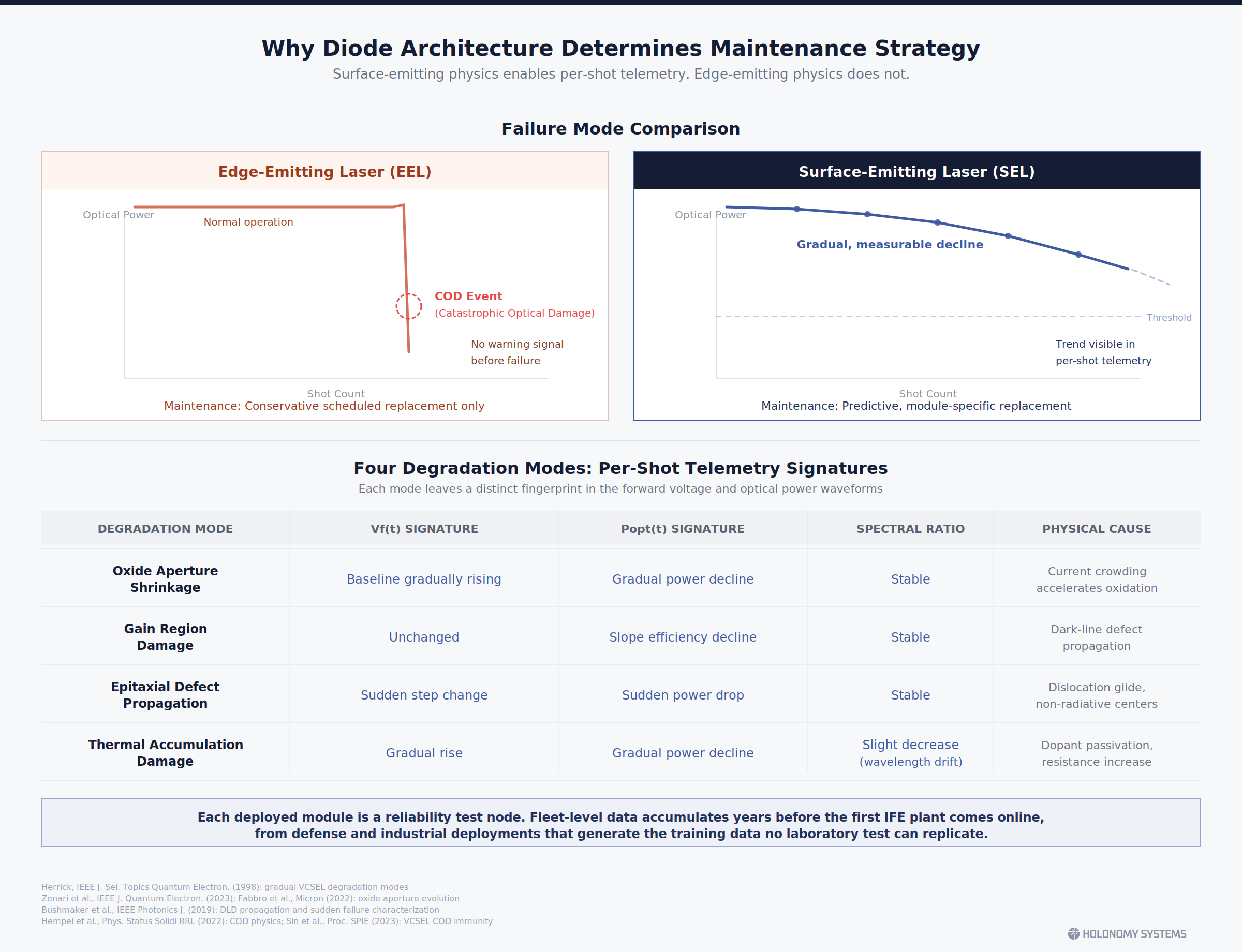
The answer begins with a physical fact that shapes everything else. Edge-emitting laser diodes fail primarily through catastrophic optical damage at the facet, a sudden-death event that is, by definition, unpredictable. You cannot build a predictive maintenance strategy around a failure mode that gives no warning. The best you can do is conservative scheduled replacement based on population-average lifetime tables.
This is where the choice of diode architecture becomes consequential. If the pump source is a surface emitter rather than an edge emitter, the physics of failure changes. With no exposed facet, catastrophic optical damage is structurally eliminated. The remaining degradation mechanisms, aperture evolution, gain region aging, defect migration, thermal accumulation, are all gradual processes that leave measurable signatures in the device's electrical and optical behavior over time. This is what makes per-shot telemetry meaningful: the physics of the surface-emitting diode allows degradation to be observed and tracked rather than merely endured.
The Photon Brick captures these signatures at every pulse. During each shot, the module records the forward voltage waveform and the optical power waveform at high time resolution, alongside die temperature, drive current, cumulative shot count, and a spectral stability indicator. These are not averaged readings. They are per-shot snapshots that reveal how the device is changing. A gradual rise in forward voltage at constant current can indicate oxide aperture evolution. A mid-pulse droop in optical output can indicate gain region degradation. A step change in voltage suggests defect propagation. A correlated drift in both voltage and spectral ratio points to thermal accumulation damage. Each mode leaves a distinct fingerprint.
Now consider the scale. A commercial IFE plant with a diode-pumped solid-state laser driver will contain on the order of tens of millions of individual pump modules, delivering roughly 50 GW of peak diode power at repetition rates of 10 Hz or higher. At that scale, bench testing and scheduled block replacements are physically impossible. What a fusion developer receives instead is a per-module health record that updates with every shot, plus fleet-level analytics that flag specific modules approaching performance thresholds. The maintenance decision shifts from "replace every N shots" to "replace this specific module during the next planned window, because its degradation trajectory indicates it will cross threshold within M shots."
There is a compounding effect that matters for the IFE timeline. Holonomy's nearer-term markets in defense and industrial laser applications will generate millions of real-world degradation data points years before the first fusion plant comes online. Each deployed module is a reliability test node contributing to the fleet-level degradation model. By the time IFE developers need to qualify pump modules for billion-shot operation, the predictive models will have been trained on an operational dataset that no laboratory accelerated-life test can replicate. The telemetry is not an added feature. It is the mechanism by which the reliability advantages of surface-emitting physics can be translated into an operable maintenance strategy at fusion scale.
Scaling of laser diode manufacturing is often mentioned as a challenge to laser inertial fusion energy companies which rely on this technology. What's the scale and price targets that have to be achieved and where are we now? How will Holonomy Systems bridge this gap?
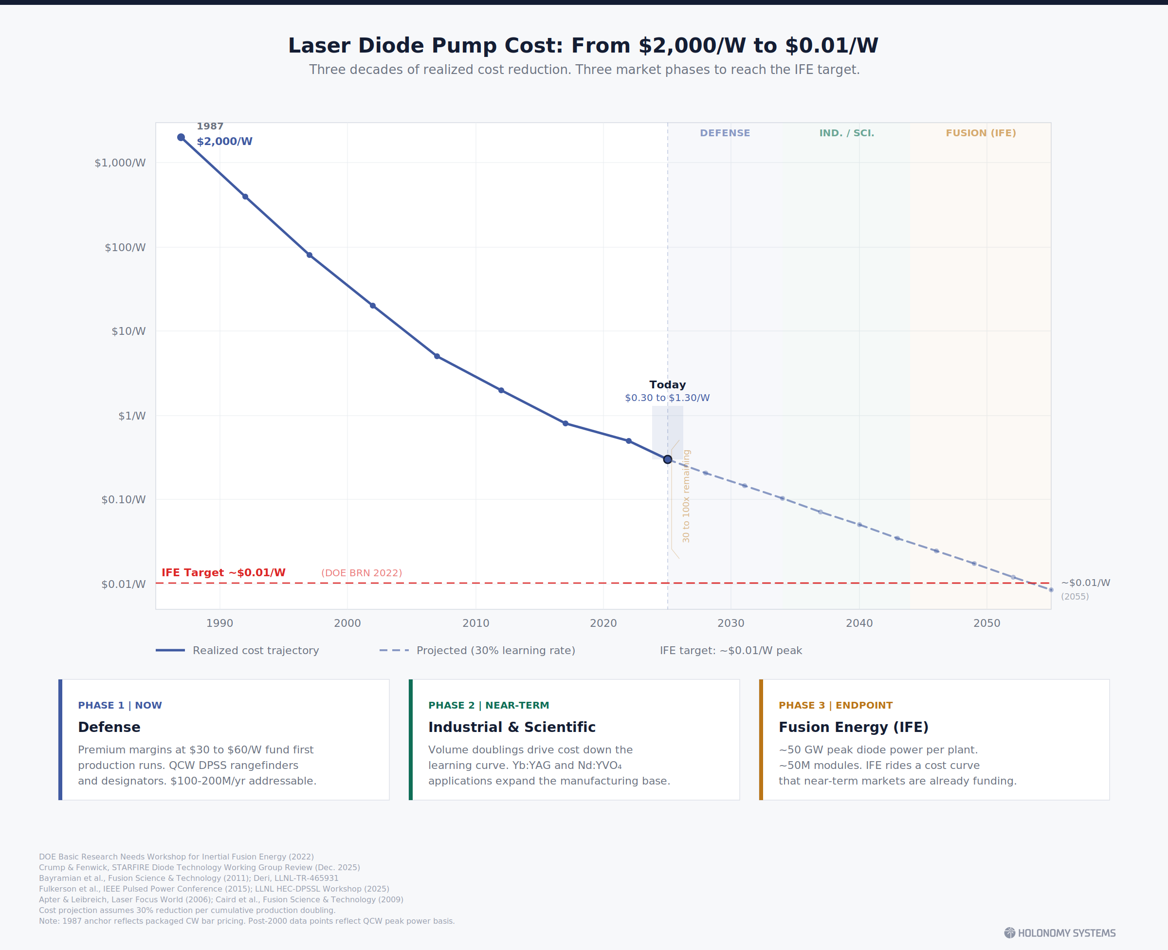
The target is well established. The 2022 DOE Basic Research Needs Workshop set it explicitly: diode pump costs need to reach approximately $0.01 per watt of peak power for IFE to close economically. Today, high-power QCW laser diode bars sell in the range of $0.30 to $1.30 per watt. That is a gap of 30 to 100 times. A single IFE plant requires on the order of 50 GW of peak diode pump power, roughly 50 million diode bars, which represents a significant multiple of current global annual production. In 1987, the same technology cost $2,000 per watt. Three orders of magnitude of cost reduction have already been achieved. The question is whether a credible path exists for the remaining 30 to 100 times.
I believe the path exists, and it runs through three structural forces. But I also want to be honest about the challenges, because this audience understands the difference between a pitch and a technical assessment.
The first force is a generational shift in the underlying diode architecture. The industry has optimized edge-emitting laser bars for four decades. That optimization has been extraordinary, but the fundamental geometry of an edge emitter creates inherent packaging complexity: asymmetric beams requiring multi-element optical correction, facet degradation as the dominant failure mode limiting peak power, and one-dimensional bar formats that constrain stacking density. Surface-emitting architectures, VCSELs and the emerging class of photonic crystal surface-emitting lasers, offer a structurally different starting point. Circular symmetric beams reduce or eliminate beam-shaping optics. The absence of exposed facets removes the primary sudden-death failure mechanism. Wafer-level testing becomes possible before singulation. Two-dimensional arrays enable higher fill factors in a given footprint.
This is not a mature technology. The honest assessment is that surface-emitting pump diodes today trail edge emitters in wall-plug efficiency by 15 to 20 percentage points at key wavelengths, and in brightness by an order of magnitude or more. But the trajectory is accelerating in ways that were not true even three years ago. In 2024, a Chinese research group published a multi-junction VCSEL achieving 74% power conversion efficiency under short-pulse conditions, approaching the long-standing edge-emitter record of 76% at room temperature. Israel's SCD, a joint venture between Rafael and Elbit, is leading a national VCSEL consortium while simultaneously serving as an industry partner on the Iron Beam laser defense program. The U.S. Army issued a 2025 SBIR solicitation specifically for photonic crystal surface-emitting lasers as pump sources. In Japan, Kyoto University has demonstrated 50-watt single-mode PCSELs with brightness comparable to fiber lasers. These are not laboratory curiosities. They are national-scale bets by serious defense and energy stakeholders that next-generation diode architectures will matter.
The second force is packaging industrialization, and this is where the diode architecture shift directly enables cost reduction. According to the December 2025 review by Crump and Fenwick, who co-chair the STARFIRE Diode Technology Working Group, packaging costs constitute well over 50% of the total diode stack cost. The precision processes involved, bar-to-submount soldering, fast-axis collimator alignment, thermal stack assembly, remain largely manual. Surface-emitting architectures simplify this problem structurally. A circular beam eliminates multi-element collimation. A 2D chip format is compatible with standard semiconductor pick-and-place tooling. Wafer-level burn-in replaces bar-level screening. The packaging step that dominates the cost structure becomes amenable to semiconductor-grade automation for the first time.
This is exactly where Holonomy operates. Our Taiwan subsidiary sits within the world's densest advanced packaging ecosystem, the same infrastructure that packages the most advanced semiconductors on the planet. We are applying that packaging discipline to a process the laser industry still performs by hand.
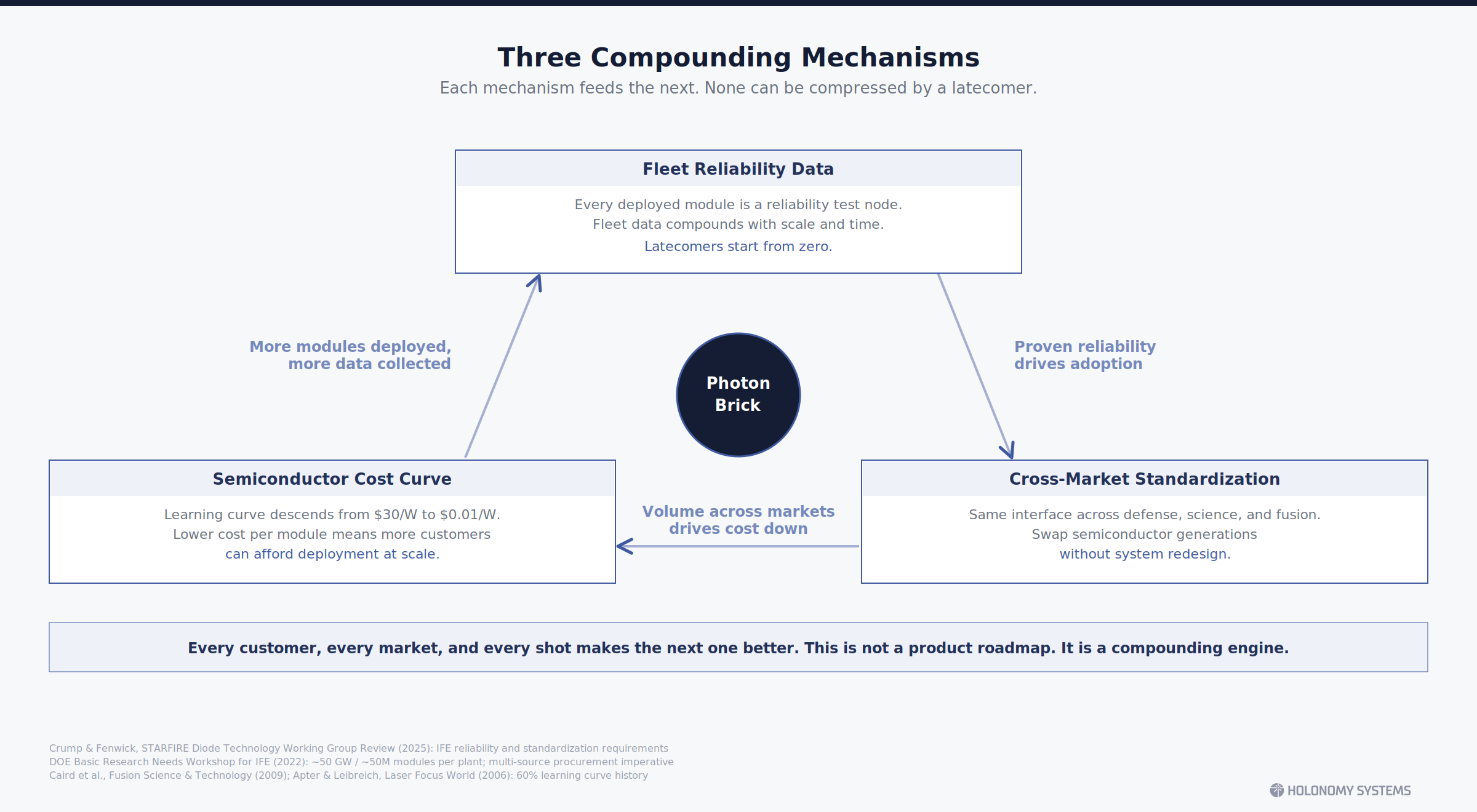
The third force is market sequencing. The cost gap from $0.30 per watt to $0.01 per watt cannot be closed by fusion demand alone, because fusion demand does not yet exist at scale. The learning curve needs intermediate markets that fund the early doublings of production volume. Defense directed energy programs pay premium margins for the first production runs. Industrial and scientific laser applications extend the curve through volume. Each market funds the cost reduction that opens the next market. Fusion is not a separate bet requiring a separate cost breakthrough. It is the natural endpoint of a cost curve that near-term customers are already funding.
These three forces reinforce each other. Next-generation diode architectures simplify packaging. Simplified packaging enables automation. Automation lowers cost. Lower cost opens larger markets. Larger markets fund further optimization. Holonomy sits at the intersection: we are building the packaging platform that translates semiconductor innovation into system-deployable modules, funded by a market sequence that reaches fusion without requiring fusion to go first.
Holonomy Systems operates with a U.S. entity handling IP and ITAR compliance and a Taiwan subsidiary providing advanced packaging at lower cost. How does that structure work in practice when serving fusion energy customers, and how do you manage export control requirements as fusion programs become more internationally distributed?
From the customer's perspective, the structure is invisible. A fusion developer interacts with a single commercial interface: they specify a module, they receive a module, they get a standard digital telemetry stream. Which legal entity manufactures the hardware, which jurisdiction it ships from, how export classifications are managed: all of that complexity is resolved inside Holonomy, not passed through to the customer.
Behind that single interface, the two entities serve distinct and complementary functions. The U.S. entity holds all intellectual property, manages export classifications, and serves as the contractual counterparty for programs subject to U.S. export controls. The Taiwan subsidiary operates the advanced packaging manufacturing line under the U.S. entity's technical direction and IP governance.
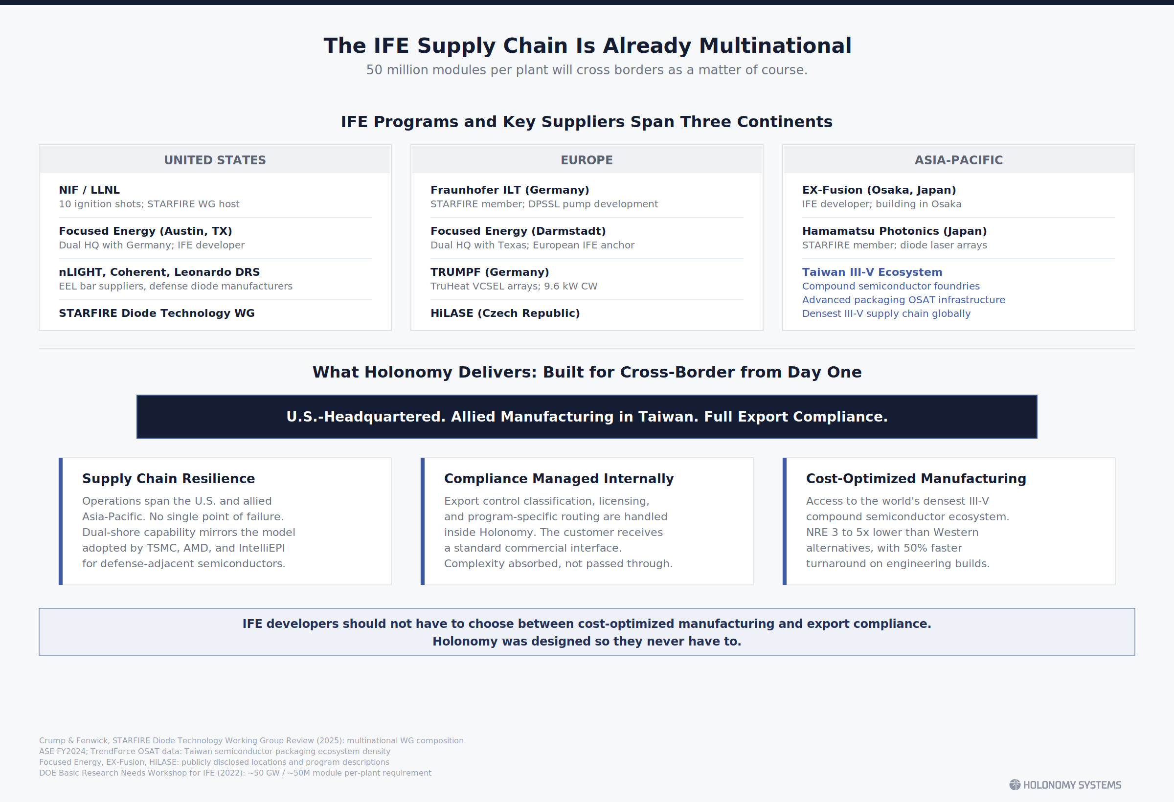
Why Taiwan is not a cost play alone. Taiwan hosts one of the world's most concentrated III-V compound semiconductor ecosystems, anchored by the largest III-V foundry globally. The advanced packaging supply chain that serves the global semiconductor industry, precision die-attach, sub-10 micron alignment, high-volume thermal management, is exactly the process technology that laser diode module manufacturing requires. We are not offshore-outsourcing a mature process to a lower-cost jurisdiction. We are accessing a uniquely capable manufacturing base that does not exist at equivalent density or capability anywhere else. The 50 to 60 percent cost advantage is a consequence of that ecosystem density, not the reason we chose the location.
On export controls specifically: fusion energy components are not inherently ITAR-controlled. The relevant considerations depend on the specific technology, its classification under the EAR or ITAR, and the end-use program. We maintain classification determinations for our products and work with qualified export counsel. The dual-entity structure gives us the flexibility to route each program through the compliance path that fits its requirements, whether that is a U.S. defense program requiring domestic manufacturing, or a commercial international fusion program where Taiwan manufacturing provides both cost and logistical advantages.
This matters because the fusion supply chain is already multinational and will only become more so. The STARFIRE Diode Technology Working Group includes Fraunhofer ILT in Germany and Hamamatsu in Japan alongside U.S. companies. Focused Energy operates in both Texas and Darmstadt. EX-Fusion is building in Osaka. As these programs move from laboratory demonstrations to pilot plants, their supply chains will cross borders as a matter of course. Most laser companies today are structured for a single domestic market. They will face the same cross-border questions eventually, but they will be solving them reactively. We designed for it from the start.
Holonomy Systems is positioned as platform-neutral, sitting between diode suppliers and system integrators without competing with either. As fusion programs move from pilot devices toward commercial plants, how do you expect that positioning to hold up, and what does the long-term commercial relationship with an IFE developer look like?
The positioning strengthens as fusion scales, for structural reasons that go beyond our own strategy.
At pilot scale, a fusion developer might tolerate sourcing pump diodes from a single vertically integrated laser company: buy the bars, the packaging, and the system from one supplier, accept the lock-in, move fast. At commercial plant scale, tens of millions of modules operating continuously for thirty years, single-source dependency becomes an unacceptable risk. Most utility-scale energy technologies have moved toward qualified multi-source supply chains as they matured. Fusion will not be different.
What makes our positioning durable is not neutrality as a principle but the compound advantages that accumulate from occupying the packaging layer at scale. Three mechanisms drive this.
The first is the data flywheel. Every Photon Brick deployed in the field generates per-shot degradation data: forward voltage waveforms, optical power transients, spectral drift indicators, thermal signatures. As installed base grows, this aggregate dataset becomes a fleet-level degradation model that no competitor can replicate without equivalent field deployment. For a fusion developer operating tens of millions of modules, the difference between population-average lifetime tables and module-specific predictive maintenance is the difference between a viable power plant and an unmanageable maintenance burden. The data flywheel compounds with every module shipped, and it starts accumulating long before fusion, in defense and industrial deployments that generate the training data years ahead of the first IFE plant.
The second is standardization as infrastructure. The Photon Brick defines a mechanical, thermal, electrical, and digital interface that decouples the pump module from the system above it. For a fusion developer, this means qualifying multiple surface-emitting diode suppliers without redesigning the pump architecture. For a diode manufacturer, it means access to system integrators without building a proprietary packaging line. The more participants adopt the interface, the more valuable the standard becomes, and the harder it is to displace. This is not lock-in through contract. It is lock-in through ecosystem adoption.
The third is the natural direction of the company's own evolution: deeper into the semiconductor, not wider across applications. The physics of the learning curve tells us that tighter integration of the diode and the packaging creates compound cost advantages that separation cannot achieve at scale. The packaging layer and the semiconductor layer share thermal interfaces, optical interfaces, and electrical interfaces. The deeper you understand one, the more efficiently you can co-design the other. As volumes grow and the manufacturing base matures, the question of where the module boundary expands becomes an economic inevitability rather than a strategic choice.
For IFE specifically, this trajectory points toward Holonomy's role in developing next-generation surface-emitting pump diodes optimized for fusion driver requirements: wavelengths matched to specific gain media, pulse formats matched to specific repetition rates, reliability profiles validated by fleet-scale operational data. The packaging platform we build today is the foundation for the semiconductor development that IFE will eventually require. The layer you standardize is the layer you eventually need to own more deeply.
The strongest evidence that this positioning endures comes from the incumbents. Every major laser company has the technical capability to standardize the pump module layer. None has built a standardized, instrumented module around surface-emitting architectures, despite decades of opportunity. The reason is structural: standardizing the module would open their packaging to competition, and adopting surface emitters would cannibalize their edge-emitting product lines. Their incentive is to keep the module buried inside the system. Our incentive is to make it a standalone, interchangeable product. That misalignment between incumbent incentives and market needs is built into the economics of vertical integration, and it persists as the market scales.
To learn more about Holonomy Systems, contact Jim Chiu at [email protected] or visit their website